Clocking scheme redesign
IDT has a new clock crossbar that would better serve AFC: https://www.idt.com/products/clocks-timing/clock-distribution/fanout-buffers-dividers-and-multiplexers/8v54816-16-port-bi-directional-m-lvds-clock-cross-point-switch
This could substitute ADN4604 with improvements. Greg, Tom Wlodkowski and the LNLS team discussed to reach the following setup:
tclka
tclkb
tclkc
tclkd
wr clock
fmc1 clk2 bidir
fmc1 clk3 bidir
fmc2 clk2 bidir
fmc2 clk3 bidir
RTM
fpga clock
fmc1 clk1 m2c
fmc1 clk0 m2c
MGT113 (FP2/AMC P2P)
MGT116 (FMC1 and RTM)
MGT213 (FMC2 and RTM)
Activity
FCLKA is the PCIe and other fabric clocks, in this case, it would be routed directly to the FPGA (MGT216, for example).
It has no use going back to the backplane, as it is already available from the MCH. Also it has not any particular use being routed to the RTM or FMC, as it does not carry any application signal, (for example, machine clock for coherent sampling). Its only use is with the fat pipe signal, which could be carried to the same MGT as it (MGT216 is the best candidate now).
As far as we know, we don't have any use case scenarios bigger than 350MHz clock. In our BPM application, we actually only transmit around 16MHz, an integer factor of the storage ring accelerator frequency, and use this as a reference to recover clock in the FMCs. A higher frequency clock could come from the RTM, also tied from the machine frequency. Most applications that must distribute synced clocks (such as timing receivers, which the AFC surely can also double) may use the same technique.
To add to the issue: the new clock switch is bidirectional, with every I/O individually addressable for direction and termination. This eliminates issues with buffers (such as the problem with FIN1101 in #1431), but most important, reduce greatly the jitter for routed clocks. Also, eases board layout, reduce the number of mounted components and buys us more real state on the board. It will take some work, but I do think it is worth it.
FCLKA is used as machine clock in LHC, at least in CMS detector.
http://iopscience.iop.org/article/10.1088/1748-0221/8/12/C12036/pdf
This isn't a problem for FPGA firmware as GTP reference clock can be used like a normal clock input buffer, but still leaves open question how to distribute this signal to FMC/RTM)(side note: in CMS infrastructure PCIe is still available on FP1, but uses asynchronous clocking with 100/125/250 MHz reference clock sources mounted on AMC module; this is somewhat more problematic, but still perfectly valid usage mode for PCIe - I've tested that it also works in AFC/AFCK if 125 MHz WR PLL is used as local PCIe reference)
I agree that having FCLKA as PCIe reference clock is important, but I can easily find other use-case scenarios
AMC13... I forgot about it.
So, the old switch was 16 inputs by 16 outputs, proposed one is 16 I/Os. This means we must make some compromise, and FCLKA was the most obvious one, as it was not supposed to be an application clock in the original MTCA architecture.
Routing it to the clock crossbar means we lose an I/O. Here's the breakdown on the proposed list above:
Required to receive/send app clock to backplane:
tclka
tclkb
tclkc
tclkdSource of "clean" clock when AFC is a timing receiver:
wr clockSending/receiving app clock to outside the crate:
fmc1 clk2 bidir
fmc1 clk3 bidir
fmc2 clk2 bidir
fmc2 clk3 bidir
RTMSo the FPGA can receive any clock needed to the MRCC, for e.g, sync data receiving:
fpga clockSo FMC1 may host a WR D3S:
fmc1 clk1 m2c
fmc1 clk0 m2cClock recovery for receiving clock from different inputs:
MGT113 (FP2/AMC P2P)
MGT116 (FMC1 and RTM)
MGT213 (FMC2 and RTM)Maybe two QUADs could share a single clock ref input pair? MGT116 and MGT213 would receive clocks, plus the MRCC? This would free an extra I/O, we could use for the PCIe.
Why we just don't give assembly options for rarely used clocks?
As it is already done with GTP links.
For CMS use case or some other non-obvious application, there can be just capacitor or 0R jumpers.
Anyway the board need to be customized for certain application in terms of GTP assignments the same approach can be applied to clocks.
We have jitter troubles in GSI with this ADN approach due to stubs on some lines. IDT chip solves them nicely.The bidirectional clocks are really messy with the ADN: you must have buffers, deal with terminations, enable/disable then and will inevitably add some jitter. Also, the phase noise on the IDT seems way lower than the ADN. This also allows us to avoid the FMC clock bypass.
On the Si571, Tom and I discussed (I believe Greg discussed with Tom at the same time), and actually, the white rabbit would work better with Si571. So, we could drop the CDCM, and the Si571 stays. If the board is not working as a timing receiver, it will be available for other functions.
fmc2_clk0_m2c, fmc2_clk1_m2c would be routed directly to the FPGA. It is a loss of flexibility, but having one FMC being able to send clock directly to the switch should fit most applications.
FCLKA and clock to GTP216 as an assembly variant is ok to me. They would actually be the same assembly, because, if you intend to use PCIe, you will probably want the FCLCKA routed to the GTP216.
I took a step back and I think this clock circuit is getting too complicated, again.
I'd like to avoid proliferation of assembly options.
I believe that it was exactly abundance of assembly options that created these trace stubs (mentioned by Greg) in the first place.Gustavo Bruno wrote:
> What about a clock source directly connect to the FPGA? Si570 assembly option that connect directly a the GTP216 clock input, for example. This would free a clock switch IO and avoid stubs.That would solve a problem for FPGA side. But in case of FMC with JESD204B chip you would also want to distribute this reference clock to ADC chip.
> But in case of FMC with JESD204B chip you would also want to distribute this reference clock to ADC chip.
Actually, in this case, the board with the chip (FMC or RTM) should send the clock to the clock switch, not the other way round.
I will answer your mail in the AFC list, I'm pretty sure we can find a good common ground with a minimum of assembly variants.
I think it is time to revive this discussion and try to achieve consensus.
From LNLS perspective the original proposal made by @gustavo.bruno and @twlostow on the issue description is still valid. The simplification proposed by @Greg on this thread concerning assembly variants for rarely used configurations is also fine with us.
@abyszuk, has anything significantly changed from your side since 3.5 years ago?
@msowinski, shouldn't we move this issue to the milestone %AFC v4.0? From the comment on #92 (closed) I suppose the IDT clock switch is still alive on WUT's plans.
Edited by Daniel Tavares@Greg , which IC did you suggest at the meeting for the clock switch? The most recent one, with bidirectional I/Os.
Edited by Gustavo BrunoYes, the same we use in AFCZ design https://github.com/elhep/AFCZ version with A suffix must be used because it has greatly improved performance - much lower crosstalk between clock channels
changed milestone to %AFC v4.0
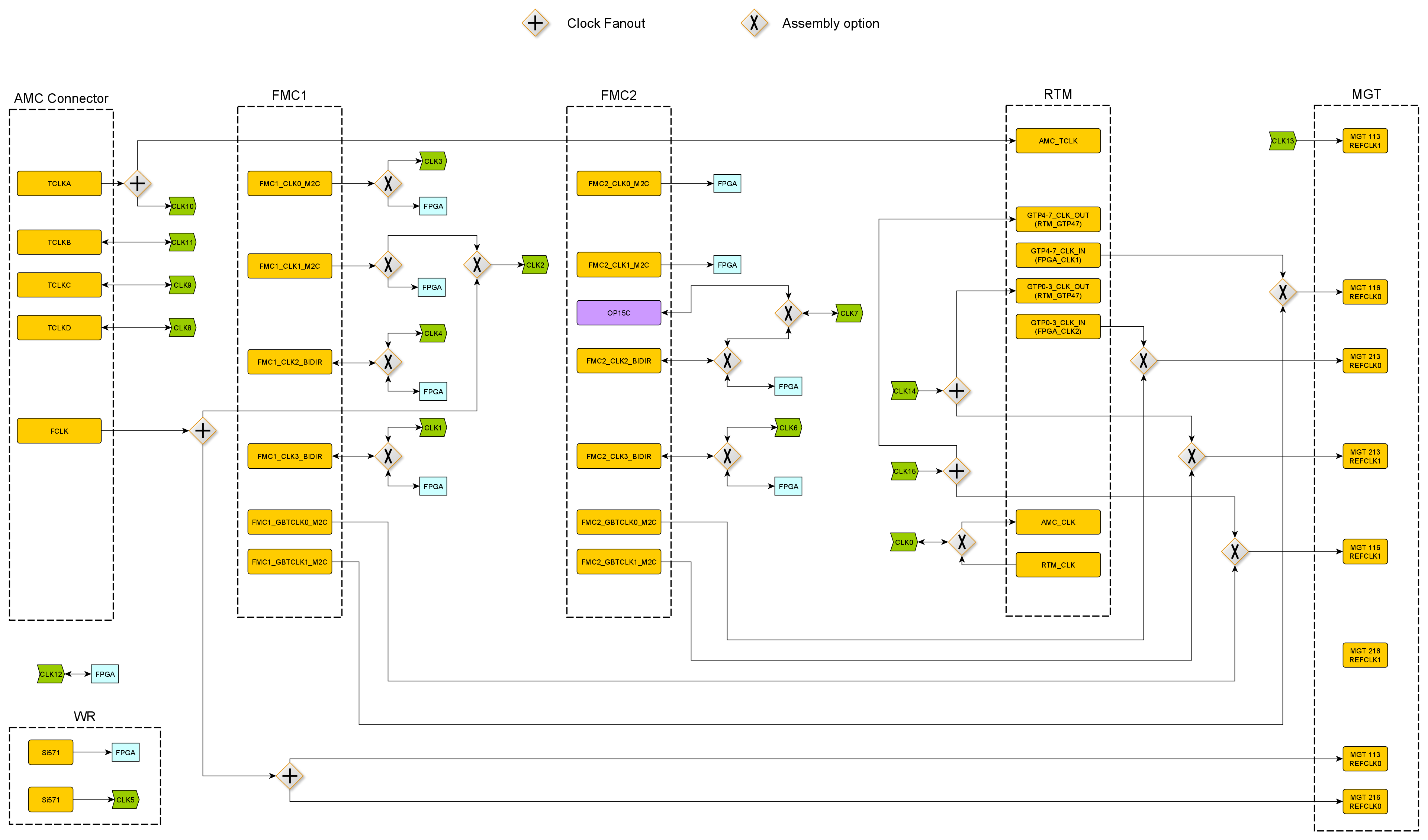
@tprzywoz mage a schematic that represents proposed clocking tree:
 I was about creating a separate issue for that clocking tree but it would be incomplete without this discussion so let's continue here.
mentioned in issue #18 (closed)
Thanks for keeping it here, this is a very complicated issue and the discussion history is very helpful. I myself had to take some time to properly understand what 2016 Aylons wrote. Guess I could have been clearer.
I suppose these mux are redrivers or buffers, right? Or are they actually demuxes? In the case of the Mux2, it would make sense to be a demux, because than you could select in the * betweein it and FCM1_M2C_1, which I suppose is a clock option. I got a bit confused here, to be frank.
This Boot_CLK line from the WR is really needed? For LNLS, the 20MHz clock not only suffices, but is a better system clock as it is fixed and more readily available (WR clock, which we could discuss separately, is often a variable clock that must be properly set, and will dynamically change).
If we're trying to be fully compatible with MTCA.4.1 RTM D1.3 (and I think this is a good idea for a universal carrier like AFC), maybe we could have a better use of the RTM_CLK (which is called CLK_EXT in AFC nomenclature -- do not confuse with AMC_CLK, labeled RTM_SYNC_CLK in AFC), which is going to UF.L connectors in v3.1.
Since now the clock switch has bi-directional ports, it seems good and easy idea to have an assembly option for either routing AMC_CLK or RTM_CLK to the clock switch. I think ideally we should have both routed, but clock switch ports are scarse resources and we don't have an application in mind right now. So, just "muxing" AMC_CLK and RTM_CLK by assembly option seems a good compromise with (hopefully) very low price in terms of routing.
Just to give a bit more context, this is the mention to those clocks on DESY RTM recommendations:
"The signal (AMC_CLK1+,AMC_CLK1-) provides typically a clock from the AMC to the μRTM and (RTM_CLK1+,RTM_CLK1-) vice-versa. The (AMC_TCLK+, AMC_TCLK-) signal offers a long-term stable timing signal, splitted from the TCLKA signal, to provide e.g. RESET signals to clock sections on the μRTM."
I'm looking at DESY RTM recommendations, it would be best to check direclty in the MTCA.4.1 specifications.
What is the real usage of FCLK on GTP 113 refclk? Couldn't we hardwire FCLK to GTP 216 only?
@abyszuk was the main contender to that idea, but his last comment a few days ago seems to indicate there should be no great opposition on taking that route.
Do we actually have AFCs operating together with AMC13 and depending on FCLK? If the AMC13 applications are foreseen in the long term I agree we should be careful about that. Otherwise I think we are better of sticking to use cases foreseen by the MTCA.4.1 standard. FCLK could be dedicated to PCIe usage then, which in AFC should also be served by GTP 216.
Edited by Daniel TavaresI'm wondering whether the FMC_BIDIR clocks really need to be bidirectional from the point of the view of the FPGA. It seems it can be only FPGA inputs, as shown here:

In that case the "X" of the diagram would actually be a simple derivation of the clock differential pair, tapping the bidir clocks to an FPGA input clock with 100 ohm termination disabled. Should this stub be a problem? Could we make the stub really small by placing this derivation close to the FPGA?
I see no serious use case where the FPGA could actually drive a clock and distribute it to other parts of the board.
It might be the case that I just hadn't understood what you meant by jumper switch. Is it a true jumper switch (a component) which you could statically control (using a physical jumper) enabling/disabling this derivation/stub towards the FPGA?
Moreover, in the case of the FMC_M2C clocks, could we simply use a 1:2 clock distributor where it is marked with a "X"?
Another minor issue concerning nomenclature: should we read the "MUX" blocks as clock distributors?
Edited by Daniel TavaresI went through all GTP clocks in the new scheme proposed by @tprzywoz. My observations:
-
I guess the diagram is not exhaustive for better visualization. In any case, I would like to be sure some existing options in v3.1 would still be kept in v4:
-
The RTM GTP clocks are muxed by assembly with FMC1 and FMC2 GTP clocks:
- MGT116_CLK0 can be driven by LINK23, FMC1_GBTCLK1 or RTM_FPGA_CLK1
- MGT213_CLK0 can be driven by LINK23, FMC2_GBTCLK1 or RTM_FPGA_CLK2
I suggest these options are reflected on the block diagram too to avoid confusion. This implies adding 2 GTP clocks coming from RTM towards the FPGA GTP ref. clks, muxed with FMC1_GBTCLK1 and FMC2_GBTCLK1 respectively before reaching the FPGA.
-
-
Now that we'll be completely dropping the FP2_CLK2 (which makes sense in my opinion) I think we could feed the second GTP 113 ref. clock directly from the oscillator used to generate WR's main 125 MHz. Having two independent ref. clocks on GTP 113 PLL is useful when using the 2x GbE + 2 SATA configuration for this tile. Sticking to WR's 125 MHz to the GbE seems quite natural for me, there's no need to be extra flexible here.
-
I always thought the names are very confusing. What do you think of renaming some nets? A first proposal:
-
Link01_CLK --> FLEX_GTP213_CLK
-
Link23_CLK --> FLEX_GTP116_CLK
-
FP2_CLK --> FLEX_GTP113_CLK
(FLEX means flexible - we could propose other names if this is not good)
-
-
As I already mentioned before, I propose we completely remove Mux2 and the "*" configuration and route FCLK straight to one of the GTP216 ref. clocks. The other ref. clock can be left open, I think there will be no big advantage to add flexibility here.
Edited by Daniel Tavares-
Ok, so I made a schematic including (hopefully) all assembly options. I'll update it according to conclusions from conversation here.
Edited by Mikolaj Sowinski- Indeed MUX on the schematics should be denoted as FANOUT as no muxing is going to be done there.
- BOOT_CLK is where it was in AFC v3.1, however it is driven from different source, namely Si571. This oscillator can be used with defined startup frequency so it does not need to be configured unless frequency change is required. AFAIK it can either well be 20 MHz.
-
FCLK is required for PCIe and thus it's connected to both MGT 113 and MGT 216. Both of these banks serve PCIe, however MGT 216 is for FP2. From what I remember these banks can't share clock.
-
jumper switch is an assembly variant
-
I don't think we can actually use a 1:2 distributor in case of BIDIR signals, unless we want to loose its's bidirectionality. In the suggested clocking diagram there is an assembly option to either have bidirectional clocking going to the clocking crossbar or to the FPGA.
Regarding FCLK: There is a CERN CMS use-case where FCLK is used as application clock. It justifies use of FANOUT that delivers clock to both MGT and clock crossbar. The question here is how probable is that CERN will use AFC in application using AMC113.
If we can drop AMC113 compatibility FCLK could be connected only to MGT, am I right?
DESY RTM complience (clocks): Add assembly variant connection for connecting RTM_ACM_CLK to RTM_CLK and AMC_CLK, as in DESY RTM specification
Hi @msowinski
Nice diagram! =] I 'll leave more specific question about the clock distribution tree to @danielot and @gustavo.bruno.
I'm only a bit concerned about the FPGA "boot" clock. From what I understood you are proposing the following:
- removing the 20MHz VCXO
- removing the 25MHz VCO that serves as the input to the CDCM PLL
- removing the CDCM PLL
- adding another SI571, in addition to the one already present
With this topology, we wouldn't have a fixed clock source from which to drive FPGA logic.
Using a Si571 to that purpose seems to work, but then we need to worry about keeping its OE pin always high and be sure that we are always mounting the same SI571 part number to keep the same startup frequency. It's all fine, but it just seems a little bit fragile to rely on a "dynamic" crystal oscillator for such a "static" purpose of driving the FPGA logic.
In addition, if we use this Si571 for that what would be the use of the extra flexibility of changing its frequency?
Is there another "fixed" clock source that could be used to drive the FPGA logic so this Si571 can be used for a different purpose?
This is a nice diagram! Thanks for incorporating some of our requests! I have a few more comments:
-
I still can't see a realistic use of the FCLK on GTP 113 refclk. I understand you want to allow PCIe on FP2 for secondary MCH, but this may be a highly unlikely use case of simply not possible, for a number of reasons:
- From what we learned from #65 (closed), the PCIe endpoint is only painfully usable on GTP 113. It seems painful to cope with such a suboptimal gateware design. Compilations will probably slow down and all you can get is a Gen1 if you're lucky.
- I doubt there are many users looking for redundant MCH nowadays, especially with the requirement for PCIe failover. Switching from MCH1 to MCH2 on the fly and make the software keep up with their normal functioning seems a huge challenge.
- To make the situation even more complicated: if you loose MCH1 you loose FCLK as well, there's no route from MCH2 to the AMC FCLK.
-
Concerning FCLK usage at CMS I cannot argue against, of course. We shouldn't break anyone's application unless we have a very strong reason to do so. My question here is the same of @msowinski's. Is CMS really expecting to use AFC in combination with AMC13 or any other scheme requiring the routing of FCLK to the clock tree? I doubt. From what I understood CMS (and all other CERN experiments) are moving away from MTCA and adopting ATCA only. I think the guys at BE-CO-HT could answer that. Could you check with them @msowinski?
We're ok if you want to give all these options to the user, but our current mindset at LNLS is to try to simplify the board's option as much as possible and only offer well supported and meaningful interfaces. In my opinion AFC is capable of supporting PCIe only at FP1.
Moreover, I would entirely prefer having a direct connection from a fixed 125 MHz clock (maybe the Si571 not connected to the crossbar?) in the remaining GTP 113 refclk to allow dual protocol (GbE + SATA (or any other protocol)) on GTP 113.
- Bidirectionality of course is a great feature and one of AFC "specialtys". AFC may be on of the few boards allowing to route the clock sourced by one FMC slot to the other slot! We should not lose this amazing capability. That said, I don't see much use of allowing the FPGA to be the source of the bidir clocks. FPGA clock are quite low quality for our typical purposes. We could avoid 4 assembly variants (the X's in the block diagram) if we simply substitute the X's of all FMC clk bidir by derivations of the LVDS pairs. Some buffering close to the derivation could be required if the resulting stub from the derivation to the FPGA would be a problem.
-
A quick question: is the OP15C an U.FL connector? Is it related somehow to the FMC connector or just a simple diagram error?
Some ideas:
-
To avoid loss of the birdirectionality of the AFC TCKA signal, the buffer could just tab into the LVDS line to send the signal to the RTM. No need to buffer the signal between the AMC and the clock switch if the RTM signal is .
-
If the stub is short enough, FPGA GPIOs and Clock switch inputs could share the line. Stubs up to 5cm should give around 330ps reflection, which seems to be acceptable for any signal that goes in an FPGA GPIO. We could always simulate this issue in HyperLynx. If needed, we could just place a buffer at the FMC<->Clock switch line, making the FPGA only an input, but I believe the stub wouldn't be a problem.
-
@lerwys @tprzywoz Maybe we could add some fixed 125 MHz oscillator if there are any CC pins available?
@danielot I feel convinced on leaving PCIe on FP2. Regarding CMS experiment, tried but didn't get any info yet.
Moreover, I would entirely prefer having a direct connection from a fixed 125 MHz clock (maybe the Si571 not connected to the crossbar?) in the remaining GTP 113 refclk to allow dual protocol (GbE + SATA (or any other protocol)) on GTP 113.
Sounds reasonable to me since I'm convinced on leaving MGT113 PCIe.
@gustavo.bruno No, OP15C is noway connected with FMC. My mistake.
First, a bit of context from what have been discussed outside this issue: there's the intent of adding one more oscillator, fixed at 125 MHz, and use it to feed GTP 113 ref. clock. This could be used as the boot clock requested by @lerwys (via IBUFDS_GTE2 + GTP instantiation) and as GTP ref. clock for protocols like SerialRapidIO or non-White Rabbit Ethernet.
Discussing offline with @lerwys one question remained though: when we forward the clock to the FPGA logic using IBUFDS_GTE2+GTP combination, is it still usable to drive the GTP quad PLL?
Yes, take a look at figure 2-1 of UG482. REFCLK is always fed, but HROW can be fed with either O or ODIV2 of IBUFDS_GTE2. You don't need to instantiate GTP itself.
You're right. Figure 3-20 (or 4-18) is even clearer. Thanks!
Edited by Daniel TavaresI decided not to update the previous clocking diagram to express that what's uploaded is the result of this lengthy discussion. Thnaks @danielot for updating according to conclusions.
Nice! I just find it a little unconventional to use an IBUFDS_GTE2 as a regular input buffer for the boot clock. I feel this would be a bit surprising to new users, as (I think) not a lot of boards use this approach. We have been using a clock like that for an auxiliary clock, sampling slow triggers (~KHz) from the MTCA.4 backplane, feeding TCLKA to the FPGA through an IBUFDS_GTE2.
One possible suggestion. Would it be possible to change Clock Switch output 12 (CLK12) to go to the MGT113 REFCLK0 and the 125MHz oscillator directly to the FPGA? Would it hurt protocols like SerialRapidIO or non-White Rabbit Ethernet?
I see @lerwys's points here. I propose we make a final assessment about the 125 MHz clock input when we have a final proposal of the pin assignment. With the latest modifications, where we removed many FMC M2C and BIDIR clocks from MRCC pins, we should have some free MRCC inputs that could be assigned to the 125 MHz clock.
This should give a clearer interface to the user.
If it is not really possible to accommodate all these requirements, we could fallback to the IBUFDS_GTE2-only approach.
mentioned in commit c2b15c2f
It looks like clocking scheme is implemented in c2b15c2f. I did a check and it seems to be consistent with @danielot schematic. Only default assembly variants are missing but I suggest dealing with it in #124 (closed).
I will close this issue and extract 125 MHz pin assignment to separate issue as I find it more clear. If you find any bugs in the current implementation of the clocking scheme please report them in new issues.
Also renamed issue so that it's easier to find for newcomers looking for justification of design choices.
mentioned in issue #125 (closed)
If the latest suggestion of reserving GTP 116 instead of GTP 213 (mentioned on issue #124 (closed)) will be accepted, the option for the fixed 125 MHz oscillator must be moved from GTP 213 to GTP 116.
mentioned in issue #136 (closed)