Remove voltage translators for the M-LVDS inputs
MLVDS circuit could be simplyfied by using the separate receiver/driver signals from the M-LVDS and using different pins for input and output in the FPGA. This would remove the need for bus direction selection, and the FPGA gateware can just ignore the inputs when transmitting in the channel.
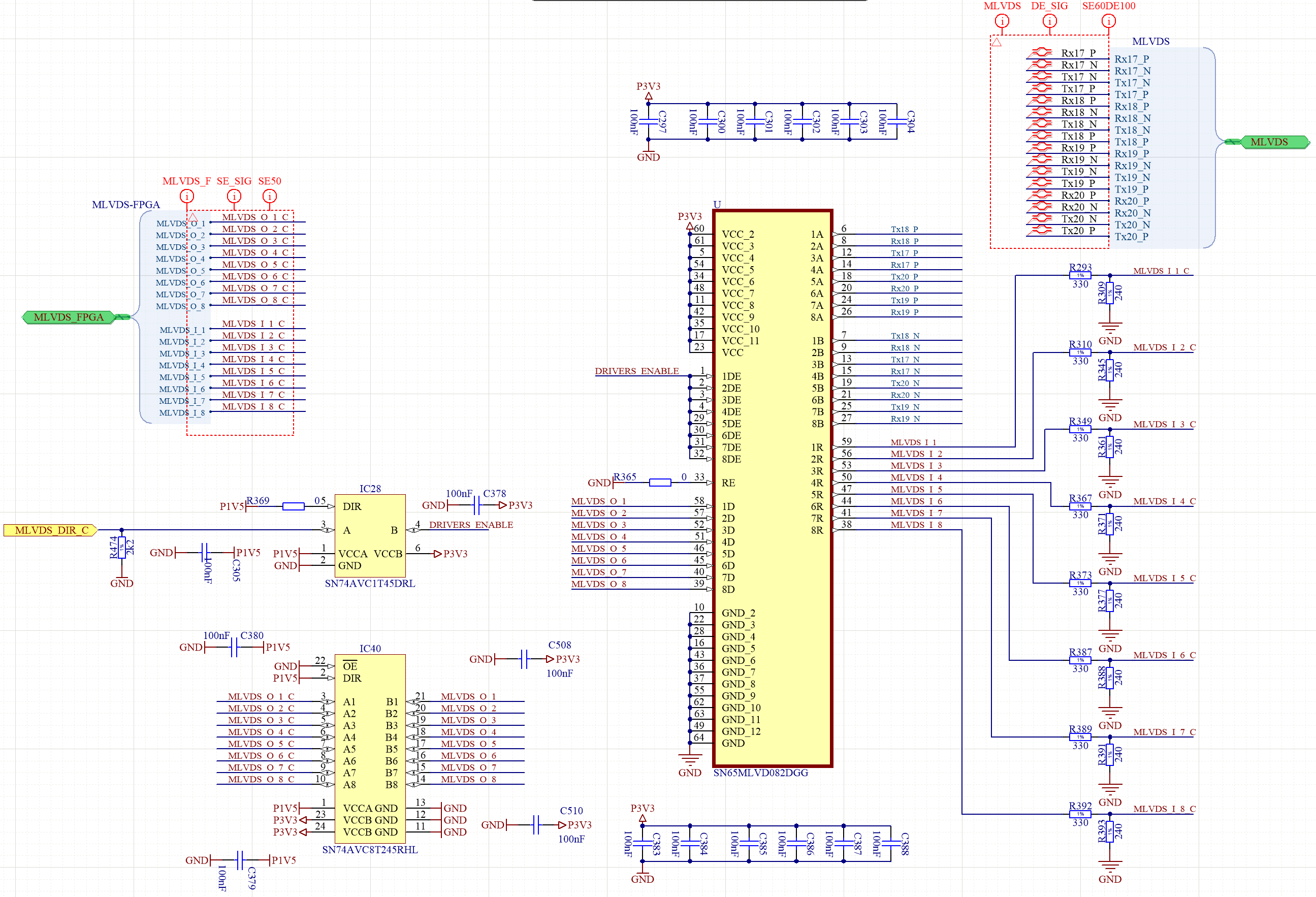
In this manner, we could employ the 8-bit SN65MLVD082 (or 080 for Type-1 receiver), allowing for better skew between channels (350ps, before it was 800ps), specially in the reception, as the voltage translation from the 3.3V M-LVDS driver to the 1.5V bank could be done by using only resistors and/or fast diodes.
The output would still need a voltage translator, but this can be unidirectional and do not need to be controlled by the FPGA. NXP 74AVC8T245 has 8 channels and allow for data rates above 200Mbps in this application. To avoid glitching the bus while programming, this translator OE could be set up as proposed in issue #87 (closed).
This would also simplify schematics, and the faster transition between receiving and sending could allow for better reuse of the bus for trigger signaling. And this modification would not need demand more pins in the FPGA. The main downside would be the lost of the ability to switch between Type 1 and Type 2 receivers dinamically, as the 8-pin MLVDS options have only one receiver option.
Activity
Let me add a little bit more context here. Discussing with colleagues at FRIB we learned that AFC M-LVDS circuitry could be improved for timing-sensitive applications (such as those found in FRIB) if 2 new conditions could be satisfied:
-
Provide an option (dynamic or by assembly variant) of fail-safe Type-2 M-LVDS tranceiver. This can be done on SN65MLVD040 via FSEN input, but this pin is currently not connected on AFC v3.1.
-
Skew between M-LVDS channels below 0.5 ns (ideal) or 1 ns.
A third requirement is already fulfilled: operate at rates around 100 Mbps. The current circuit should allow 250 Mbps.
What @gustavo.bruno suggests seems to meet those more stringent requirements in an elegant way. After discussing with FRIB we see no reason why not use Type-2.
Could we all converge to Type-2 for the default AFC assembly?
Edited by Daniel Tavares-
Currently, we have selectable direction translators in MLVDS lines. The idea is to have single-direction translators, just in the TX. We would keep using the same number of FPGA pins, the direction selection being changed to TX lines. I don't see why we would want an extender - we have currently about 40 GPIOs unused in the FPGA.
assigned to @tprzywoz
Great. The selection between Type-1 and Type-2 is easily done by selecting which IC to solder, SN65MLVD080 or SN65MLVD082, as you probably are already aware of.
Now, the question about whether this should be an assembly option or not, that's a good question. Since we're trying to minimize the number of variants, we could leave Type-1 as an "undocumented assembly option" instead of reserving one character in the part number for this.
We have no preference from our side. We'd be happy with any choice.
This is more related with timing sensitive use cases, such as those found at FRIB (Michigan University). They need lower skew and skew drifts among channels.
So, the main argument for simplifying the level translators is "timing performance", with the trade-off of losing the dynamic selection among Type-1 and Type-2.
As a side note, I don't see any advantage in the proposed solution (Gustavo's) in terms of slew rate performance. The current circuit is already very fast. It should operate up to 250 Mbps, and it is hard to imagine someone would want to go beyond that. The SN65MLVD would cap to 250 Mbps in any case.
Edited by Daniel TavaresWhy would we need do drive DE and RE pins on the MLVDS if we are using separate pins in the FPGA? The RE pins can be always on (we just ignore them in the FPGA if we are sending data), and at worst the DE pins may be controlled in the same manner we control the voltage translators. Or we can just let the voltage translator off during programming as it already is and the drivers pulled.
Something went out of our radar for a while about this circuit. There were 2 hidden but important points to consider:
- To enable wired-OR functionality, which is required in LNLS use cases, we should use the FPGA to assert SN65LVD082's DE pins instead of D pins. D is fixed in HIGH. It means the bus is released when we have no signal to transmit.
So, in practical terms, we should swap D and DE circuits on the above schematics.
- The mode of operation described in (1) has a downside for timing-sensitive applications: the edge of the transmitter output when DE goes low will be slower, since it is not driven but given by the circuit capacitance. Fig. 6 of the SN65MLVD082 datasheet should illustrate this (https://www.ti.com/lit/ds/symlink/sn65mlvd082.pdf).
If high speed is required and wired-OR is not (i.e. there's only one driver on the bus), then it is probably better to command D directly while the driver is enabled (DE = HIGH).
Meeting 1 and 2 would require then 8 more pins on the FPGA (same bank) and one more SN74AVC8T.
Edited by Daniel Tavares@cogansco, since your application is very timing-senstive I think you're in the best position to answer this: would you prefer to bundle D+DE in the same bank or D+R in the same bank?
There are 16 pins on bank 32 and 8 pins available on bank 35. The true question is how to make the best use of them for the M-LVDS lines.
Edited by Daniel TavaresIn the currently proposed schematics the connections of ports A and B to AMC connector are not ordered in correspondence with the MLVDS 1-8 lines. AMC RX-TX ports 17-20 not being in order on SN65MLVD082 is not an issue, since this may be related to easing the routing, but I suggest at least R, D and DE ports follow the same order.
For instance, MLVDS_O_1 (and MLVDS_I_1) should be connected to 4D (and 4R), not 1D (1R), since it should be associated with AMC Port 17 Rx. Does it make sense?
Edited by Daniel Tavaresmentioned in commit 9098d25e
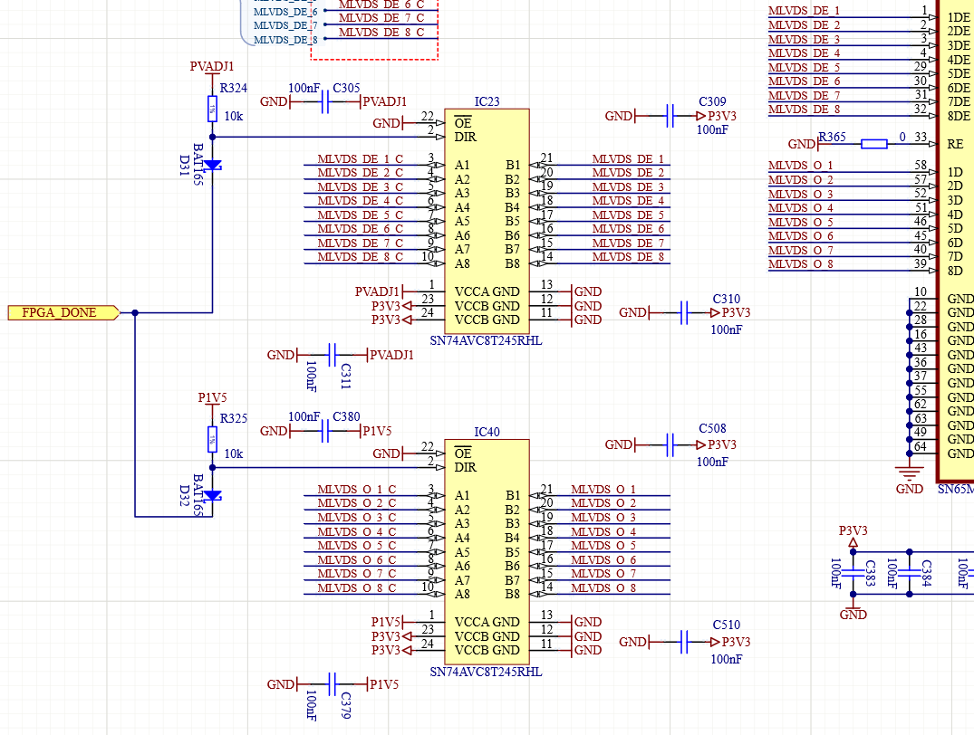
DE signals connected to bank 36. According to #87 (comment 116783): IO pin (for switching off MLVDS drivers during configuration) changed to DONE pin.
mentioned in issue #87 (closed)
mentioned in commit 0d87a553
What is the purpose of D31 and D32? Could they not be omitted or replaced with small resistor?
Edited by scott coganI see now on RC6 that all AMC ports are reverse ordered on the driver MLVDS input/output (A-B ports):
- Rx17 goes to ports 8A-8B
- Tx17 goes to ports 7A-7B
- ...
- Tx20 goes to ports 1A-1B
This is no problem at all. The choice of A-B ports must be driven by the layout.
What bothers me now is that MLVDS_[DE/I/O] signals connected to DE/R/D ports are now in reversed order too.
For better readability and to avoid confusions when operating with other AMC boards in the crate, the order we prefer is:
- MLVDS_[DE/I/O]_1 : Rx17
- MLVDS_[DE/I/O]_2 : Tx17
- ...
- MLVDS_[DE/I/O]_8 : Tx20
My suggestion: assign the AMC ports 17-20 in the way you prefer to ease routing. Make the correspondent assignment on ports DE/R/D that ensures MLVDS_[DE/I/O]_1 refers to Rx17, MLVDS_[DE/I/O]_2 refers to Tx17, etc.
Edited by Daniel TavaresWas not implemented in v4.0 and I'd keep it that way. After all it's just the matter of constraints. @danielot if you disagree feel free to reopen and assign to v4.1.
@msowinski, I suppose you refer only to my last comment (#131 (comment 117049)), that is, reording the labels.
Documentation has been an issue in the past and I think we should try to keep things as clean as possible. I do think it will pay off to do this minor fix.
changed milestone to %AFC v4.1
@msowinski @tprzywoz Is it ok if we do this?
mentioned in issue #180 (closed)
Made a #180 (closed) , so yes :-)
changed milestone to %AFC v4.0