Change SCANSTA111 to SCANSTA112
The main feature that is only present in SCANSTA112 is the Transparent
Stitcher Mode.
In this mode, the IC can be configured via hardware to skip the
addressing protocol needed, so we don't have to run a SVF configuration
file on IMPACT when programming the FPGA bitstream (the JTAG mux would
already be transparent a directed to the FPGA chain).
Another reason to perform this upgrade is that we can include the MMC in the JTAG chain, since the SCANSTA112 has 7 slots, rather than the 3 in SCANSTA111. This would allow us to program and debug the LPC17xx controllers using openOCD and Buspirate for example, as described in this link.
The addressing pins needed to put the SCANSTA112 in the Transparent Stitcher Mode should be controlled by the MMC.
More information about these JTAG switches can be found in this document from Texas Instruments.
See https://github.com/lnls-dig/afc-hw/project/ohr-support/issues/232
Activity
Changed in commit:26aa3b1b
Is this really resolved. I still see some problems:
- enabling stitcher mode by variant should also enable transparent mode (maybe replace it with a DIP switch?)
- LSPSEL[1..5] should be controlled by MMC
- RTM signals are connected to RTM_JTAG harness in reverse order
- Y101 output is just a passthrough pin, the LED will never workAs a small deficiency: SCANSTA power supply is connected P3V3. This means that in case where AFC doesn't get 12V supply, or P3V3 is not enabled it won't be possible to remotely debug MMC via AMC JTAG.
Not sure it this is a problem for you, just mentioning.Thanks for the heads up in the RTM harness, I have already corrected it.
Non-transparent stitcher mode would be the main way to use the SCANSTA from the backplane, so you should be able to configure them separately through the JTAG itself.
IMHO transparent stitcher mode, with selectable LPSEL pins, is useful for bench and JTAG-cable use. So, maybe the DIP switch instead of MMC should control transparent stitcher and LPSEL? I'm not sure if the MMC should control it, specially as it is downstream to it.
On the LED, it was a leftover I let pass. The intention was to use these pins to show which LP was selected, as it is tristated when LPSEL is not selected. Not possible, because not every output has this passthrough. Already removed it. thanks for the revision.
For the P3V3, sure, it should get its power from P3VMP, if possible. However, care must be taken to see if there's available power on this rail for it. I'll check it out.
Gustavo Bruno wrote:
> Non-transparent stitcher mode would be the main way to use the SCANSTA from the backplane, so you should be able to configure them separately through the JTAG itself.
>
> IMHO transparent stitcher mode, with selectable LPSEL pins, is useful for bench and JTAG-cable use. So, maybe the DIP switch instead of MMC should control transparent stitcher and LPSEL? I'm not sure if the MMC should control it, specially as it is downstream to it.I'm not sure it will be possible to easily use SCANSTA in any other mode than transparent stitcher.
As far as I understand it, transparent mode is the only mode in which Xilinx software (ISE or Vivado) will work.
Vadatech JSM is just a simple JTAG mux - after selecting AMC slot (which is done in quite inconvenient way BTW.) you have to use Xilinx's programmer and software to control AFC.
I don't have experience with NAT JSM, but after reading:
http://www.nateurope.com/products/NAT-JSM.html
I understand it basically works in the same way. It's just more feature complete and easier to use (e.g. select slave port via NAT-MCH webpage). But even if programming via MCH and ethernet, the XVC protocol still assumes it can talk directly to Xilinx FPGA.Or to put it another way: no matter the JSM, it's still Xilinx software talking to Xilinx FPGA which requires transparent mode.
P.S.
NAT-JSM - use of Altera FPGA in Xilinx-oriented JSM really does add some 'evil genius' twist to it :-)I believe it is possible to use the SCANSTA with IMPACT or Chipscope, with a SVF to program the SCANSTA beforehand.
If I'm wrong (I haven't tested it yet) it is possible to program, via JTAG bus, the SCANSTA to become a transparent stitcher, for any LP we would like to, after that we launch the Xilinx software. This way, the SCANSTA would be transparent until reset (naturally, it can't receive any commands while transparent). It would actually work in much the same way the IP version of NAT-JSM switch, only one more layer deep.
This may sound convoluted, but my intention was to have this as a backup for programming the MMC in case of a catastrophic firmware failure. It would also be a faster way to reprogram the FPGA than the HPM in operation.
In the end, if you are plugging cables directly on the board, there's no reason not to setup which device you want to access through the DIP switch. And if the board is away, programmin the SCANSTA via JTAG sounds reasonable.
Of course, I haven't tested this yet, but we could try using the SCANSTA111. Do you have any experience with it?
Also, I really like the intrusion of an Altera device in the backside of a MTCA crate. :c)
I completely agree with DIP switch approach in case of direct access.
The approach you suggest in JSM case isn't much different from what we do now with SCANSTA111. You have to insert SVF preamble or run IMPACT/Vivado script to set up jtag mux.
But I see it clearly now - yes, your idea seems to be the best one. Direct control via DIP switch if connecting directly or quick SCANSTA setup in JSM case.
The only task to solve is remote reset of this mux. It can be done via so called five-high TMS reset. Probably doable with openocd or urjtag, I don't know if it's possible to control Vivado at such low level.Hey @Greg , what about this solution for the JTAG? How do the AFCZ JTAG circuit compare to this?
We used SCANSTA112 in AFCZ and it caused many problems with the reliability of JTAG chain. We used in in a mux mode only, controlled by MMC. In the new revision we will use multiplexers like on Xilinx devkits. The muxes will be controlled by FMC and RTM present pins with the possibility of manual override by MMC. In AFCZ SCANSTA was controlled by MMC which added RTM to the chan when it was inserted. The Vadatech JSM causes more problems than actually solves. It requires manual toggling of the switch. NAT does not use SCANSTA, its switch is controlled by MCH where JTAG maser is implemented.We had a lot of issues with dying SCANSTA chips. TI does not support them anymore because it is not their product. They only produce silicon. THat's why they were unable to help us resolve the issue. On AFCZ one SCANSTA also died. It behaved normally but the signal was no longer passed in any mode. The users complain a lot about this SCANSTA chips. The idea to debug MMC in crate is not very useful. MMC is supplied from management power. The JSM is supplied independently. This will break the JTAG chain frequently, also causing issues with MMC being supplied by JTAG lines. I don't see a use case. It's much easier to connect the JTAG probe locally, without a need to modify the debugger commands to tackle with SCANSTA. Debugging MMC usually involves observation of I2C lines using scope or analyzer; it also needs access to the front panel handle so it's hard to make it remotely. My recommendation is the following:
- use a few muxes controlled by MMC
- MMC senses RTM and FMC presence pins and then sets desired JTAG configuration
- JTAG switches can be overridden by IPMI commands manually
this circuit does exactly what we need, but it's working without any user intervention. When USB debug cable is removed, the AMC becomes JTAG host. When payload power is off, the AMC is connected to MMC. This enables remote MMC update.
 When payload power is on, the FPGA is connected to either USB JTAG or AMC JTAG.
This is working, we have it implemented on one of AMC boards.
When payload power is on, the FPGA is connected to either USB JTAG or AMC JTAG.
This is working, we have it implemented on one of AMC boards.marked #95 (closed) as a duplicate of this issue
I implemented @Greg 's circuit with a few changes to ensure compatibility with 2 FMCs:
- Added the third NC7SZ157P6X
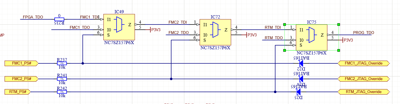
- PROG_TDI is now directly connected to FPGA_TDI. I needed free pin of SN74LV541 (there was already second free pin) to fanout TMS and TCK signals to 4 devices (AMC FPGA, RTM, 2 x FMC)

R210 R212 and R436 are default not mounted.
- Added the third NC7SZ157P6X
changed milestone to %AFC v4.0
Solved in c961a747
mentioned in issue #114 (closed)
