 Vasco Guita
Gateware and software
Download gateware and software
Software (LM32 firmware):
https://www.ohwr.org/project/wrs-low-jitter/uploads/a7b99ebe575502924dc210006451dcbe/rt_cpu.elf
Gateware (18 ports):
https://www.ohwr.org/project/wrs-low-jitter/uploads/855d42369c507be50c0bc198419017de/scb_od.bin
Building software (only for developers)
The LM32 software can be download using Git, type the following command:
git clone git:https://www.ohwr.org/hdl-core-lib/wr-cores/wrpc-sw.git
cd wrpc-sw
git checkout mattia-wrs-low-jitter
make all
The resulting binary (rt_cpu.elf) must be copied in the /wr/lib/firmware directory of the WR Switch
Building gateware (only for developers)
You can download the source of the gateware using the following commands:
git clone -recursive git:https://www.ohwr.org/white-rabbit/wr-switch-hdl.git
cd wr-switch-hdl
git checkout mattia-wrs-low-jitter
cd ip_cores/wr-cores
git checkout mattia-wrs-low-jitter
The external clock input provided by the WRS Low Jitter daughterboard is
processed by a DDMTD block. The DDMTD can be sensibile to the internal
clocks inside the FPGA. To avoid any noise coupling the gateware has
been built using a PBLOCK constrain to exclude any logic around
clk_i_d0 and clk_i_d1 of the ddmtd_with_deglitcher.vhd DFFs (the
ones that are used to demodulate the input clock). Additionally, these
DFFs are manually placed.
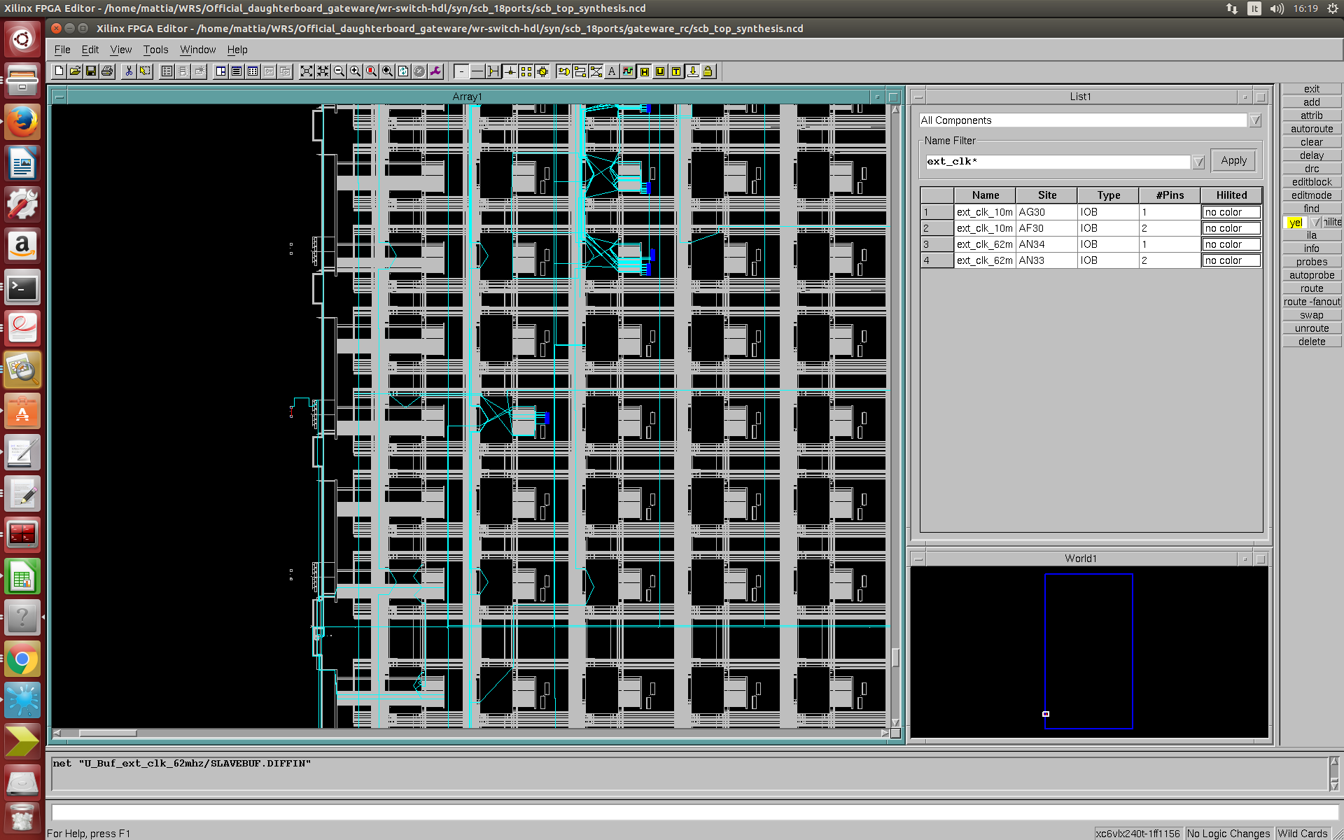
Unfortunately the PBLOCK constrain is sometimes ignored by MAP due to a
bug. A correct image of the FPGA must be check with FPGA editor (looking
for ext_clk_62* lines). A correct image is as follows:
https://www.ohwr.org/project/wrs-low-jitterhttps://ohwr.org/project/wrs-low-jitter/uploads/feec6b61c0f539a1cdc818fe92bf6b07/fpga_editor.jpeg
Note that around the central SLICE there's no logic. Be sure also to check inside the SLICE. Only clk_i_d0 and clk_i_d1 logic can be inside the SLICE. A correct image of the FPGA has been uploaded to check it with FPGA Editor at https://www.ohwr.org/project/wrs-low-jitter/uploads/144934155312242548d53855bea21950/scb_top_synthesis.ncd
Validating the gateware in GrandMaster mode
The published gateware has been validated by manually moving the phase
set-point at 100ps steps to check if any jumps were detected while
running in GM mode (using 3120A). None of them were detected.
A working GM should have a Modified ADEV at 1s of less than 5E-13. If a
value greater than that if measured, check with 3120A if some jumps were
detected.
If you see some jumps like these ones then you ahave a noise
coupling.

Check with FPGA editor if any external logic has been placed around the
DDMTD DFFs.
This kind of noise is probably due to ground bouncing. Since the nearby
DFFs are switching using clk_sys, which is phase related to the clock
provided by the WRS Low Jitter, if you're unlucky the external clock
edge is near the clk_sys edge, providing this kind of jumps. Check on
the FPGA Debug console Setpoint value if the Setpoint value, Setpoint
mod 8192 is below 2000 or above 6000. If yes, reboot the switch and
retry to measure it when it's around 4000.
The provided gateware doesn't show this kind of effect, however an easy
workaround (in case you keep to experience this kind of noise with a
rebuilded gateware) is to keep resetting the PLL of the WRS Low jitter
board until the external clock is not near the clk_sys clock edge. This
is very feasible modifying spll_external.c FSM. This has not been
implemented since on the provided gateware the jump effect was not
visible on any 100ps steps.